Written By Dr. Jim Tzeng on 08/07/2020
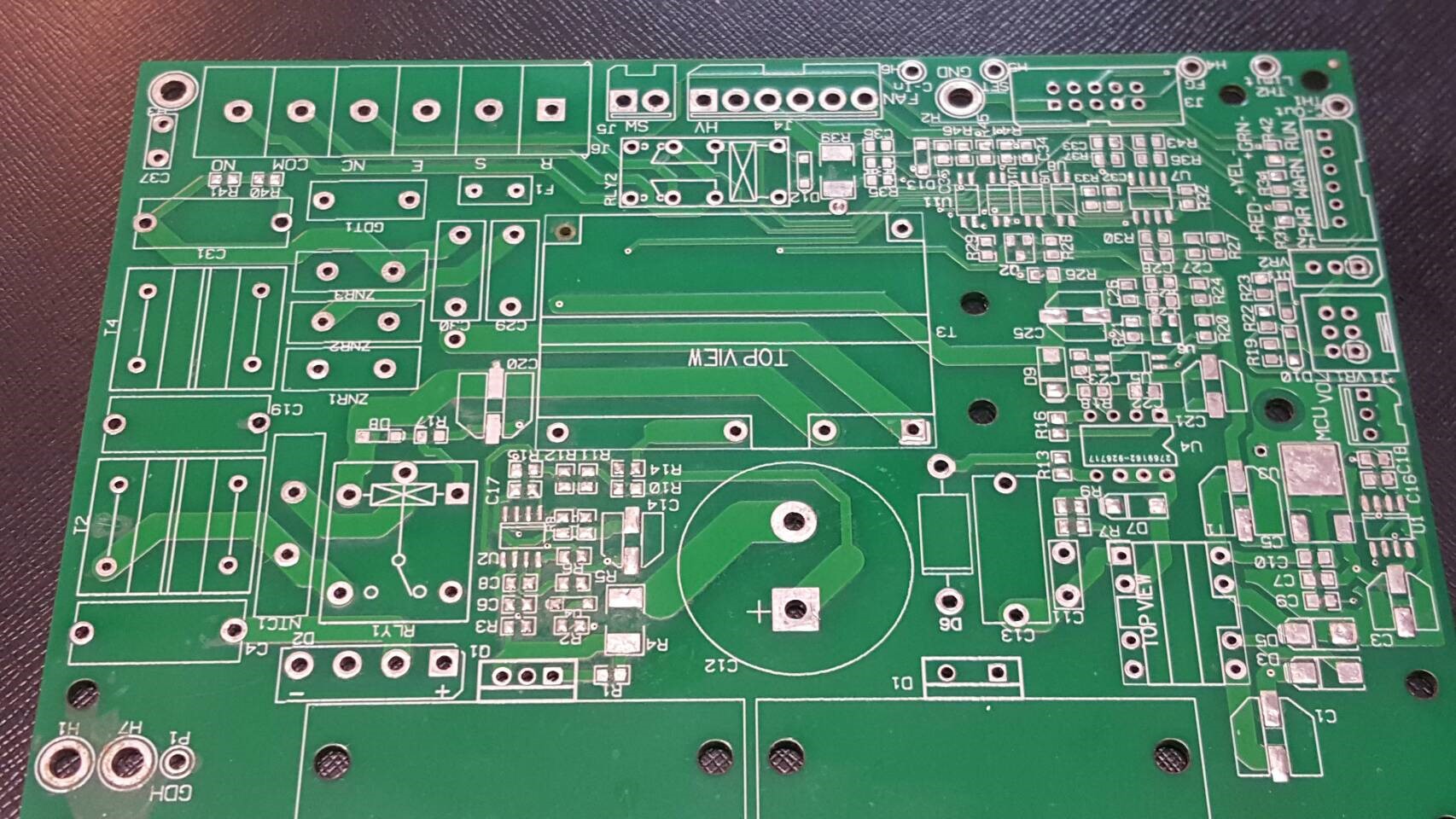
The printed circuit board (PCB), also called printed wiring board (PWB), circuit board, and circuit card, is the central item in electronic devices. A PCB is essentially a mechanical and electrical platform where electronic components are mounted and matrices of electrical traces are built into the board. The PCB technology was developed and came into practical use after World War II. In the 1950s and 1960s, the single-sided board was the most popular version of PCBs and is still in use today for low-cost consumer electronics. The PCB architecture of electronic systems has replaced old-fashion “point-to-point wiring”.
In the early 1970s, the PTH (plated-through holes) technology was developed to make reliable and consistent copper deposition and electroplating on inner surfaces of holes. This allowed circuits to be placed on both sides of PCBs for more convenient connection and double-sided boards overwhelmingly became the industry standard. As component densities and circuit complexities increased, the multilayer board was introduced by the mid-1980s and accounted for the majority of the PCB production. A PCB with mounted electronic components using surface mount technology (SMT) and through-hole technology (THT) are conventionally called a printed circuit board assembly (PCBA). Over years of development and progress, the PCB technology in conjunction with comprehensive assembly methods (e.g., SMT and THT) has become a predominant architecture in the electrical and electronic industries.
I. Types of PCBs:
Fundamentally, a bare PCB board is made by laminating copper foils onto a dielectric plate or sheet substrate. The dielectric substrate is in general a composite material of resin, with or without particulate fillers, and reinforcement fibers, woven or not. The dielectric substrate is often called laminate for the means and construction of the substrate system. Based on the degree of flexibility and the nature of substrates, PCBs can be classified as rigid PCBs, flexible PCBs, and flex-rigid PCBs. While the rigid PCB is the most popular type, flexible and flex-rigid PCBs have gained their shares by the demands in the fast-growing markets of cell phones, mobile/handheld electronics, touch panels, and displays in recent years.
1-1. Rigid PCBs:
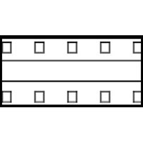
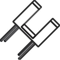
Rigid PCBs are the PCBs with rigid laminates. They can be single-sided, double-sided, or multilayer. A single-sided PCB consists of only one copper layer on one side of the laminate. Similarly, both sides of the laminate of a double-sided PCB are bonded with copper foils. On a double-sided PCB, the circuits on two sides of the board can be connected through vias or plated through holes (PTHs). A multilayer PCB can be various stack-up combinations of double-sided PCBs, copper-prepreg layers, and laminates. For complicated electronic devices of higher component density, multilayer PCBs are normally used for accommodating more components and complex circuit systems.
For example, most LED light strips use single-sided PCB and LED driver boards are typically double-sided. Computer motherboards and PCBs for cell phones are most often of 8~16 layers or more. Recently, the PCB technology has also been applied to various innovations of semiconductor packaging. An example is the viable Chip-on-Board (COB) technology, of which a system packaged of multiple chips delicately interconnected on a single substrate.
1-2. Metal-Core PCBs (MCPCB):
The dielectric substrate or laminate is normally poor in conducting heat. Therefore, for better heat dissipation, the electrically insulated substrate of PCBs is replaced by metals. The copper foil is then bonded to the metal base by a thin layer of thermally-conductive dielectric adhesives (typically thermal set plastics). PCBs with metal plates is called metal-core PCB or MCPCB. Metals of choice are various grades of aluminum and copper alloys. The MCPCB is mostly single-sided. Growing technological efforts are ongoing for reliable and cost-effective manufacturing schemes of the double-sided MCPCB.
1-3. Flexible PCBs:
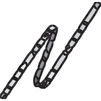
Flexible PCBs, as named Flex-PCBs or FPCs, use flexible plastic substrates, such as polyimide and polyester, instead of rigid laminates. Flex-PCBs can be used as a standalone copper-clad foil or be laminated to thin stiffener films. The flex-PCB can be made by the photolithography, similar to that of rigid-FPCs. On the other hand, it can be made by fairly different “wet” processes, e.g., silkscreen printing of conductive pastes on flexible plastic substrate and then cured or baked.
The flex-PCB is a convenient and cost-effective replacement for wire harnesses for its weight, thickness, and flexibility advantages. One of the major advantages of using flex-PCBs is that they can be easily folded into desired shapes, conformed to a confined space, and tightly packed in devices of stringent form-factor constraints.
Additionally, flex-PCBs permit constant flex or bending as encountered by design as the normal usage of some electronic devices. Relatively speaking, the flex-PCB is more tolerant to moisture, corrosion, heat, solvent, and contamination in the field.
1-4. Rigid-Flex PCBs:
Rigid-flex PCBs are a hybrid construction of rigid and flexible PCBs which are physically combined in a single construction. For one, rigid-flex PCBs are compact in size because the rigid and flex sections of the PCBs are bonded in situ inside the boards. Combining rigid and flexible PCBs into single boards allows for more concise designs for less board size, package weight and attachment processes.
II. Properties and Characteristics of PCBs
A PCB is essentially a stack-up of copper clad laminates. Electrical currents and signals travel through copper traces and plated-through holes (PTHs). Traces are made by selectively removing portions of the copper foil. PTHs are created by deposition and electroplating of copper layers on the walls of holes. PTHs connect circuits on different layers of PCBs.
2-1. Copper thickness:
Thickness of copper foil is customarily expressed by its areal weight in ounce per square foot or Oz/ft2. The areal weight of 1 Oz/ft2 (customarily referred as 1 Oz copper) is equivalent to the thickness of 1.344 mil (thousandth of an inch) or 0.034 mm (34 µm). The laminate of 1 Oz copper is the most commonly used boards. Boards of 0.5 Oz (17 um) and 2 Oz (68 um) copper are also common for the consideration of electrical impedance, thermal dissipation, overall thickness, or cost. Foil over 3 Oz is often referred as “heavy copper” for the circuits of high current and/or high watt. The flex-PCB typically has thinner copper liner for better flexibility and durability.
2-2. Trace Resistance:
Resistances of traces are controlled by their thickness, width, and length. The individual total resistances of each and every trace must be kept significantly low to minimize the line voltage loss. As the common practice, power and ground traces are set wider, if board space permits.
2-3. Substrate:
Substrates are dielectric composite materials. The composites contain electrically insulated plastics (e.g., epoxy, polyester and polyimide) and a reinforcement component (e.g., woven or non-woven glass fibers and paper). In some cases, particulate fillers (e.g., ceramics and titanite) are added into resin as dielectric modifiers. Factors of cloth weaves, thickness, and percentage are used to tailor desired overall thickness and dielectric characteristics. IPC4101C primarily uses fiber, resin, and composite ratio for the designation of laminates (e.g., FR-4, CEM-1, G-10, etc.) The table below lists a few IPC4101C category codes of some commonly used laminates.
There are various dielectric materials that can be chosen for different electrical properties. Commonly used laminates include FR-4 (Flame Retardant), FR-1, CEM-1 (Composite Epoxy Materials), CEM-3, BT and Teflon. Thermal expansion is an important property to be considered, especially when used to mount ball grid array (BGA) and bare-die packages. Resin with glass fiber generally offers best physical and dimensional stability. Among all, FR-4 is the most commonly used material for its well-balanced performances and CEM-3 is the alternative for cost reduction.
The reinforcement materials can be woven and non-woven. Woven reinforcements are cheaper, but come with higher dielectric constants. Also, the spatially nonhomogeneous nature of woven fibers may introduce a little bit of local variations in electrical properties because of uneven distribution of the weave pattern. Laminates of non-woven reinforcements and low-to-no reinforcements are more suitable for high frequency and analog applications because of their lower dielectric constant.
III. Some key properties of laminates are briefly introduced below:
3-1. Glass transition temperature (Tg):
The glass transition temperature represents the demarcation when the phases of plastics switch between a rigid (glassy) state to a softened state. Plastics of higher Tg signifies that the material does not get softened until exposed to higher temperature. At temperature exceeding Tg, the laminate softens with a significant increase in expansion and deformation. Deformation of laminates poses potential harms to PCB’s electrical and mechanical integrity. Repeated soldering or high-temperature exposure can cause catastrophic failure. Therefore, thicker PCBs require substrates of higher Tg.
3-2. Thermal expansion:
The coefficient of thermal expansion (CTE) is measured by the ratio of the increase in length by the margin of temperature difference. The CTE is expressed in ppm per degree Celsius (ppm/oC or µm/mºC). Expansion constraint by the woven glass makes CTE along the (X-Y) plane significantly lower than that in the through-sheet (Z) direction. Typically, CTE in Z direction should be around 70 ppm/oC or lower.
3-3. Thermal Conductivity:
Thermal conductivity represents the ability of a material to conduct heat. It is measured as the rate of heat transferred through a unit area at a given length by a given temperature differential, and is expressed in W/mºC. Thermal conductivity of PCB substrates is normally around 0.2~0.8 W/mºC, significantly lower than that of the copper foil. As a rule of thumb, heat generated by electronic components on PCBs is dissipated mostly through copper layers. Layout of maximum copper coverage is beneficial for high power components.
3-4. Dielectric constant:
Dielectric constant signifies the signal propagation speed and usually decreases with the increase in frequency. The frequency dependence may introduce undesirable phase distortion in wideband applications. More importantly, laminates need to be properly selected and designed for achieving sufficient impedance matching required by high-frequency communication and analog transmission.
3-5. Dielectric breakdown voltage:
The breakdown voltage determines the maximum voltage difference imposed on both sides of the PCB laminate. When exposed to the breakdown voltage or higher, the board may arc and eventually get scorched and disrupted.
3-6. Loss tangent:
Like dielectric constant, loss tangent is an important properties to be considered when selecting laminate materials for high-frequency applications. It represents the loss of energy, absorbed by the board laminate, from the signals.
3-7. Moisture absorption:
All PCB laminates absorb water more or less. Absorbed water may results in deterioration of PCBs in many different ways, such that the board may get cracked, popcorned or delaminated, and shorts/opens occur between pads and traces. Care must be taken on board storage and de-moisturization prior soldering. After a period of long-time storage, proper baking procedures of PCBs and substrates are required before any manufacturing processes.
IV. Relevant safety regulations, specifications, and standards:
IPC2222: Design standard for rigid PCBs
IPC2223: Design standard for flex PCBs
IPC4101: Specification for PCB base materials
IPC6011: Class definition of PCB quality levels
ISO9001: Quality management system (QMS)
ISO14001: Environmental management system (EMS)
ISO13485: Medical Devices Quality Management System
IATF16949: QMS for the automotive sectors
UL746E/F: Standard for laminates used in PCBs and dielectric films
UL796: Standard for PCBs in general
UL94: Flammability
RoHS: Restriction of hazardous substances
REACH: Registration, evaluation, authorization and restriction of chemicals
Mil-PRF-50884/31032/55110: Performance specification
V. Design and definition of PCBs for manufacturing:
PCB design begins as an EE designer passes circuitry, BOM (bill of materials), and PCB requirement (stack-up, impedance, thickness, etc) to a PCB layout engineer. The task is to complete and arrange component interconnection based on the circuit design. Nowadays, locations of components and traces are”laid out” or drawn by using commercially available computer-aided design (CAD) software. These CAD data, conventionally stored in Gerber files which numerically describes images, drawings, and features of each PCB layers. Gerber data are standard inputs to all CAM device reading images. In addition to Gerber data, descriptions of PCB materials, processes & finishing, and output requirements need to be specified for PCB fabricators:
- Type of material (e.g., FR4, CEM3)
- Standards of specifications (i.e., ICP Class, UL94)
- Solder pad finish (e.g., ENIG, HASL, OSP)
- Solder mask requirements (e.g., brand, color)
- Panelization of boards (e.g., pattern and number)
- Silkscreen requirement (e.g., brand of ink, color, size)
Test & inspection requirements (e.g., Test Points, fly probing, e-test)
VI. Common PCB defects
Solder Bridging is one of the common defects of PCB abnormality due to poor solder mask layout. Solder bridging shorts circuit and may jeopardize printed circuit board assembly and cause permanent damage by overloading components and traces. It is important to have sufficient space between solder pads
Plating Voids may be caused by a gap or uneven coating of copper on the wall of plate-through-holes. Plating voids result in open circuit of PTHs and vias connecting traces from two separate layers.
Popcorning is most likely caused by excessive water absorption of laminates and poor surface bonding or coating processes. Popcorning can often cause trace breakage and circuit failure.
Physical Damage includes deformation, breakage, and misalignment of PCB stack-up. The physical anomalies may lead to a variety of functional failure which may not be easily identified and trace back to the origin of the root causes.


